Professor UEDA Kenji

- Posted
- Fri, 01 Apr 2022
日本語版はこちら/Click here the Japanese version
Introduction
|
 |
Laboratory Introduction Video
Research
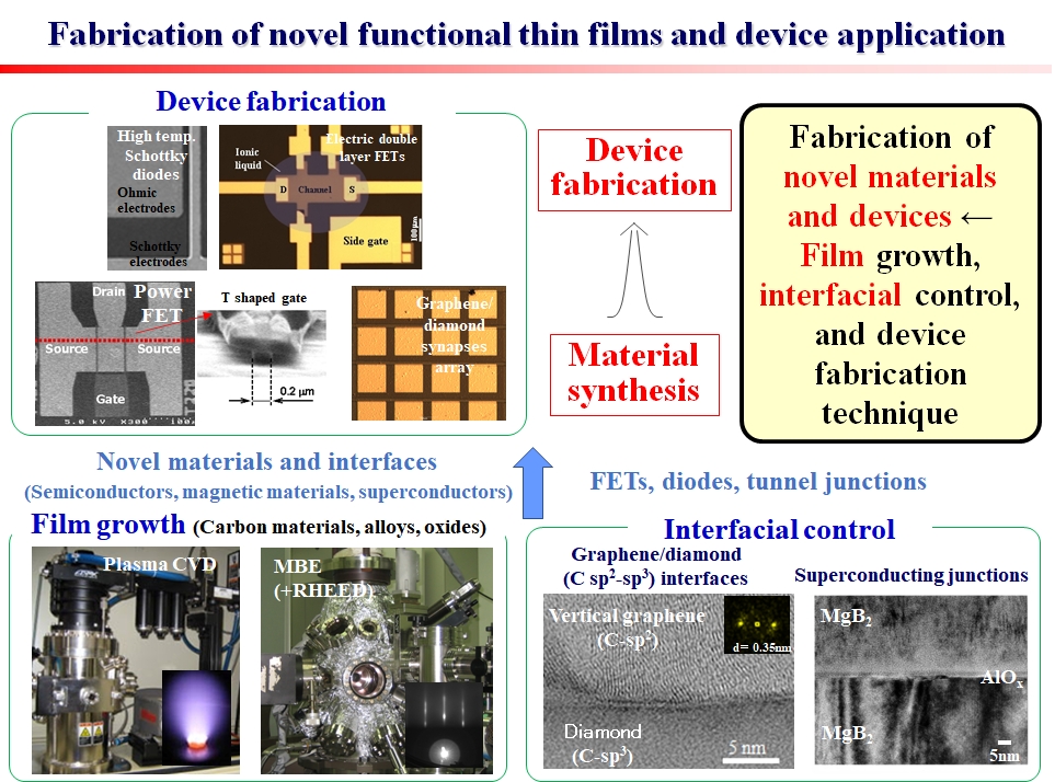
Intelligent Semiconductor Engineering
Thin films are used in various purposes such as optical functional films, magnetic films, semiconducting devices, etc. It is not too much to say that these functional thin films manage not only present information society but also our life. In our laboratory, we have been developing novel thin films, especially novel brain mimic materials and devices, that can innovate our information society, by using thin film growth and interfacial control technique.
Recently, we have mainly been fabricating novel materials and devices by combining graphene and diamond semiconductor films, which are typical inorganic carbon materials. Followings are our recent research topics.
・Fabrication of novel brain-mimic optoelectronic memory devices using graphene/diamond semiconductor junctions.
・Reservoir computing using graphene/diamond semiconductor devices.
・Development of high-performance graphene/diamond semiconductor power devices.
・Fabrication of ultralow power consumption devices by using Bi based topological materials
|
 |