Professor SHIMURA Takayoshi

- Posted
- Mon, 01 Apr 2024
日本語版はこちら/Click here the Japanese version
Introduction
|
Laboratory Introduction Video
Research
Semiconductor Materials and Device Engineering
Advanced material analysis using synchrotron radiation and development of germanium based light receiving/emitting devices for next-generation optoelectronic integration
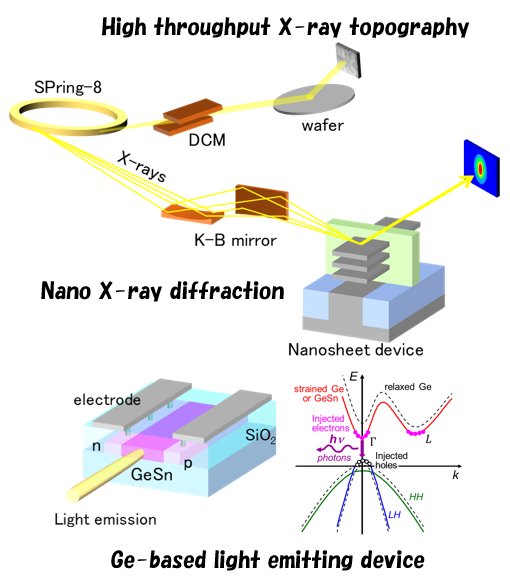
Japan is promoting projects to revive its semiconductor industry. The Japanese government is providing financial support to semiconductor companies to boost domestic semiconductor chip production. I aim to contribute through the advanced material analysis using synchrotron radiation of SPring-8, and development of germanium based light receiving/emitting devices for next-generation optoelectronic integration.
|
 |