OMINATO Yuya, Assistant Professor
Aiming for a Main Role in Next-Generation Devices: “Electron Spin” and “Two-Dimensional Atomic Layer Materials”
My field of expertise, “condensed matter physics,” is a discipline that clarifies the motion of particles that compose matter and elucidates the properties of matter. I propose theoretical principles for the operation of next-generation devices. My goal is to obtain research results that will contribute to the advancement of our information society. Miniaturizing and integrating electronic devices for electrical appliances such as today’s PCs and smartphones have allowed development to attain high performance, such as high speeds and conservation of energy.
However, the high performance made possible by conventional microfabrication technologies is approaching its limit. Therefore, in order to go beyond that limit and to create a breakthrough, I am focusing on the properties of electrons as magnets, called spin. In electronic devices used in conventional computers, the negative charge of electrons acts as an information carrier, but I am studying how to use electron spin as a new information carrier.
At the same time, I am also focusing on the “ultimate thin film” that is called “two-dimensional atomic layer materials” as a material for next-generation devices. For example, a two-dimensional atomic layer material called “graphene” is a sheet-like material that is as thin as one carbon atom. It is the thinnest sheet in the universe. Because graphene has a property in that the electron mobility is 100 times greater than that of silicon, which is commonly used in conventional electronic devices, it has the potential to make information processing much faster when used as a material in devices.
How to generate spin current in graphene
Computers represent all data as “1s” and “0s.” For example, “1” is represented when a current is flowing, and “0” is represented when a current is not flowing. Similarly, if the orientation of the N and S poles of spin magnetism corresponds to 1 and 0, the spin can be used as an information carrier (Fig. 1).
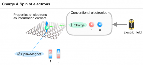
Fig. 1. Electron spin is regarded as a magnet. The N pole of the magnet corresponds to an upward orientation of 1, and the S pole corresponds to an upward orientation of 0. For that reason, the spin can be used as an information carrier by a computer.
I am theoretically researching the mechanism that generates the “spin current,” which is a magnetic flow derived from spin. It has been experimentally reported that the spin current suppresses heat generation compared to the charge current. By developing a device that utilizes the spin current, it is expected that we can attain greater power savings compared to conventional devices.
Here, I briefly describe how spin currents are generated in graphene. Affix a magnet to graphene as shown in Fig. 2. The spin is aligned for the electrons in the magnet so that the N-pole is downward. By applying a microwave to the magnet to generate magnetic resonance, electron spin starts the frame motion (precession motion) all at once. With this, the electrons in the graphene near the interface with the magnet change the orientation of the spin so that the N pole is upward. This results in the spinning electrons accumulating near the interface between the magnet and graphene, with the N pole facing upward. As the electrons with this accumulated N pole facing upward spread in the right direction in Fig. 2, a spin current occurs. This phenomenon is called spin diffusion, and it is similar to the spread of milk dripped into coffee.
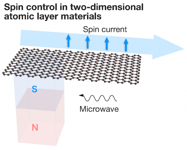
Fig. 2. Spin current occurs when a magnet is attached to a sheet of graphene (two-dimensional atomic layer material) and a microwave is applied. When the microwave hits, the electrons in the magnet start the frame motion (precession motion). Also, the electron spin in the graphene is subjected to a magnetic force, and the direction of the spin is biased at parts that touch the magnet and parts that do not. This results in spin current when electrons are moved so that the electron spin is uniform.
Combining two-dimensional atomic layer materials to develop new physical properties
In leading-edge research, efforts are being made to attain new physical properties by implementing various creative measures on two-dimensional atomic layer materials. For example, a Moiré pattern occurs when a sheet of graphene is slightly shifted and two sheets are stacked (Fig. 3). A Moiré pattern is one that occurs when there are multiple regular repeating patterns. Recent experiments have demonstrated that this Moiré pattern dramatically changes the motion of electrons in graphene. This means that a whole new field of research has been opened up in the field of material design and physical property exploration by utilizing Moiré patterns.
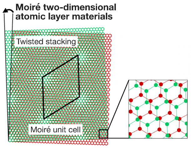
Fig. 3. A Moiré pattern is generated when graphene is slightly shifted and stacked. It can be seen by looking at the diagram, that the thin parts appear at equal intervals. The interval of this Moiré pattern is longer than the interval of the carbon atoms that compose the graphene. A two-dimensional atomic layer material with a Moiré pattern is collectively referred to as a Moiré two-dimensional atomic layer material.
In the future, I aim to explore various two-dimensional atomic layer materials, including graphene, to discover the mechanisms behind spin currents generation and new physical properties that are expressed by shifting and stacking them. Based on the results, I would like to propose the operating principle of next-generation devices.
Coverage/Constitution: Keiko AIMONO
Cooperation: Graduate School of Political Science, Waseda University, J-School