What are carbon nanotubes (CNTs)?
CNT is a material composed only of carbon atoms. It is a cylindrical structure of sheets of hexagonally connected carbon atoms. Organic matter such as DNA and protein and inorganic matter such as graphite and diamond have carbon atoms in different forms. A form of carbon, CNT was discovered in 1991, and ever since, it has been used in various fields owing to its superior properties. However, because of high production costs and difficulty in producing structures that utilize its beneficial properties, there are very few practical applications of CNT. Thus, I am developing a practical and a scalable-production method to manufacture a structure that benefits from the properties of CNTs. Additionally, I am engaged in the study of new applications of CNTs.
Advantages of CNTs
Carbon fiber, a material similar to CNT, has already been widely used. Compared to carbon fibers, CNTs have a higher crystallinity and a more regular arrangement of atoms. The high crystallinity makes it more difficult for the electrons and heat to be scattered, which results in higher electrical and thermal conductivity of CNTs. CNTs are also expected to be mechanically stronger than carbon fibers because of the high crystallinity.
Growth of CNTs
There are two main methods to produce CNTs: Physical Vapor Deposition (PVD) and Chemical Vapor Deposition (CVD).
In the case of PVD, carbon in the graphite form is the raw material. It is to be noted that both graphite and CNTs are steady substances. Graphite is heated until it reaches an unstable gaseous state, and then cooled to produce CNTs.
CVD is based on a chemical reaction. It uses chemical compounds that include carbon (mainly gas), such as acetylene and ethanol, as raw materials. The growth temperature for CVD can be lower than that for PVD as CVD uses carbon compounds as feedstocks that are less stable than graphite. Firstly, a metallic thin film (iron, cobalt, nickel, and others) with a few nanometers thickness is deposited on substrates. Then, the substrates are heated up to 800 °C in a reactor under hydrogen flow to reduce the metal films and form nanoparticles. When the carbon feedstock is introduced, the nanoparticles catalyze the decomposition of the feedstock followed by the growth of CNTs. This metal nanoparticles not only catalyzes the decomposition of the feedstock on the surface but also acts as a “mold” that defines the diameter of the CNTs.
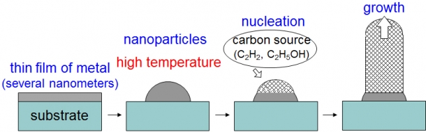
Figure 1: CNT grown using CVD method
Requirements to use CNTs in wiring
Computers and smartphones have large-scale integration (LSI) chips whose integration capacity has been improving every year with the use of smaller wiring circuits and higher electric current densities. Currently, copper is being used as the wiring material. Copper is cheap and has low resistance, but it fails at a current of around 6×10⁹ A cm-2. This paved the way to study the properties and uses of CNTs, which can withstand a current approximately 1000 times higher than copper can. CNTs have high thermal conductivity so they are also beneficial to dissipate heat efficiently.
In order to use CNTs in the vertical wiring of LSI chips, it is necessary to grow them inside a narrow well-like hole satisfying the following three limitations. The first one is to produce them at 450 °C or below. Normally, the growth of CNT requires a temperature roughly between 700 and 800 °C, but it needs to be lowered to 450 °C or below, which is the temperature maintained during the conventional manufacturing process of semiconductors. The second limitation is that the CNTs and the substrates need a good electrical contact for the current to pass. The growth of CNTs is easy on insulators but difficult on conductors (metals) because the surface energy of conductors is generally higher than that of insulators resulting in higher reactivity with catalyst metals which inhibit the CNT growth. The third limitation is to reduce the resistance of CNTs to a value lower than that of copper. This can be done by lining up a large number of CNTs as a “forest” and thus raising its density. It is important to fulfil these three limitations to produce wiring with CNTs.
Achieving the highest mass density to date with cobalt-molybdenum catalysts
In this study, I have used a combination of cobalt and molybdenum as the catalysts. Although CNTs grow with cobalt alone, I combined molybdenum to increase their density. The molybdenum is chemically bonded both with titanium (support) and cobalt (catalyst) resulting in the formation of cobalt nanoparticles with narrow diameter distribution. In addition, the cobalt nanoparticles are anchored on the substrate surface during the CNT growth. On the contrary, in the absence of molybdenum, the diameter distribution of cobalt nanoparticles become wider and they are lifted up as the CNTs grow. As a result, the CNTs do not grow straight, decreasing the forest density.
I devised an efficient method to find out the optimum thickness of cobalt and molybdenum. Since there can be numerous thickness combinations of the two metals, experimenting one combination at a time would be an exhausting task. Therefore, I devised a “combinatorial method” which can develop gradient thickness profiles of the metals on a single substrate. First, I deposited a molybdenum thin film layer that becomes thinner from left to right as shown in Figure. 2. Then, I repeated this with a cobalt layer that decreases in thickness from back to front. Thus, I created samples of both metallic films with varying thickness between 0.1 and 10 nm on a ~ 15×15 mm2 substrate.
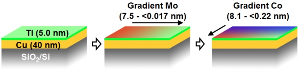
Figure 2: Development of molybdenum and cobalt films using combinatorial technique (H. Sugime, et al., ACS Appl. Mater. Interfaces 6, 15440 (2014))
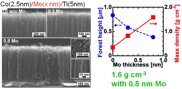 Figure 3 left: Cross-sectional images of CNTs on molybdenum films with varying thickness (0, 0.3, and 0.8 nm).
Figure 3 right: Forest height and mass density of CNTs as a function of Mo thickness The mass density of the forest reached the highest reported value in the world (1.6 g cm-3) when the thickness of molybdenum was 0.8 nm. (H. Sugime, et al., Appl. Phys. Lett. 103, 073116 (2013))
I succeeded in growing CNTs with the highest mass density reported so far using an extremely thin film (0.8 nm) of molybdenum with this technique.(Press release:American Institute of Physics) When the molybdenum thickness becomes large, the cobalt nanoparticles possibly diffuse into the molybdenum layer resulting in the failure of the CNT growth. In addition, this growth process was carried out at a temperature of 450 °C, which satisfies the first of the three limitations.
Aiming to study the growth mechanism of CNTs and to put it into practical use
A few characteristics, such as two nanotubes joining midway through the process were observed for the first time by examining the growth process of the high-density CNT forest obtained in this experiment. This can contribute to a better understanding of the growth mechanism of CNTs. Also, from the perspective of practical use, CNTs can be more easily applied to electronic devices than conventional CNTs on insulating supports. Currently, I am engaged in studying the application of biosensors for medical purposes. In the future, I would like to focus on basic research on exploring the growth mechanisms of CNTs as well as on applied research on application of biosensors, and thereby develop a more practical approach to grow CNTs.
Interview and Composition: Seiko Aoyama / Junichi Tsuchiya
In cooperation with: Waseda University Graduate School of Political Science J-School